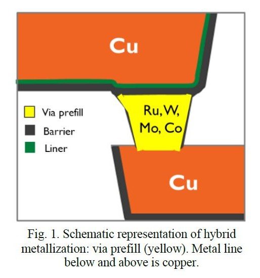
CMOS多層配線の高密度化を支えるビア電極の微細化 配線層を銅(Cu)、ビア電極(黄色の部分)を高融点金属で形成する多層配線の断面構造図。出典:imec(IEDM 2020の発表論文「Inflection points in interconnect research and trends for 2nm and beyond in order to solve the RC bottleneck」(論文番号32.2)) (クリックで拡大) 記事に戻る 福田昭,EE Times Japan