次々世代のトランジスタ「シーケンシャルCFET」でシリコンの限界を突破(後編)
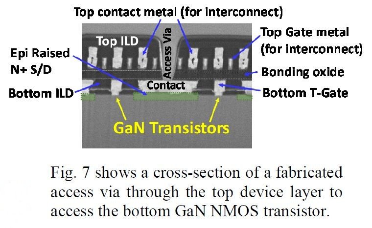
試作したシーケンシャルCFETの断面を電子顕微鏡で観察した画像。ビアを介して上下のトランジスタを接続している。出典:intelが2019年12月に国際学会IEDMで発表した論文「3D Heterogeneous Integration of High Performance High-K Metal Gate GaN NMOS and Si PMOS Transistors on 300mm High-resistivity Si Substrate for Energy-Efficient and Compact Power Delivery, RF(5G and beyond) and SoC Applications」(論文番号17.3)から(クリックで拡大)