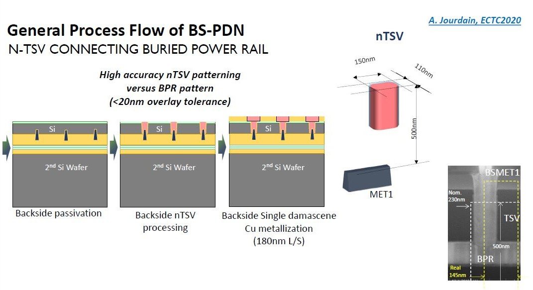
電源供給配線網(PDN)をシリコンダイの裏面に配置して電源をさらに安定化 裏面側に電源供給配線網(BS-PDN)を製造する工程(後半)。出典:imec(IEDM2020のチュートリアル講演「Innovative technology elements to enable CMOS scaling in 3nm and beyond - device architectures, parasitics and materials」の配布資料) (クリックで拡大) 記事に戻る 福田昭,EE Times Japan