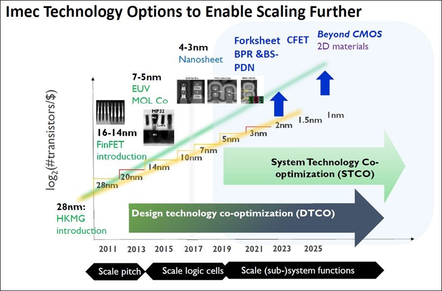
TSMCとSamsungのEUV争奪戦の行方 〜“逆転劇”はあり得るか? 図15:1nmまでのロジック半導体のスケーリング 出典:Myung Hee Na, imec, “Innovative technology elements to enable CMOS scaling in 3nm and beyond - device architectures, parasitics and materials”, IEDM2020 Tutorials 5(クリックで拡大) 記事に戻る 湯之上隆(微細加工研究所),EE Times Japan