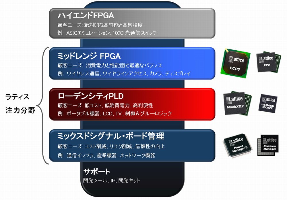
Latticeの次世代FPGAは28nmプロセスを適用、新CEOが来日会見で表明 図2 注力する応用領域と各領域に対応する製品群 出典:Lattice Semiconductor 記事に戻る 薩川格広,EE Times Japan